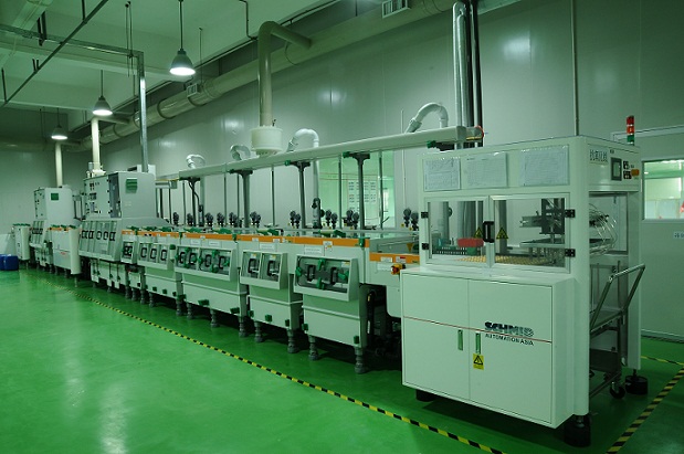
Organic Solderability Preservatives technology introduction
OSP is the abbreviation of Organic Solderability Preservatives, and also known as Preflux in English. Simply put, OSP is to grow a layer of organic skin film on the clean bare copper surface by chemical method. This film has anti-oxidation, heat shock, moisture resistance, in order to protect the copper surface in the normal environment no longer continue to rust (oxidation or vulcanization, etc.); However, in the subsequent welding high temperature, the protective film must be easy to be quickly removed by the flux, so that the exposed clean copper surface can be immediately combined with the molten solder into a firm solder joint in a very short time.
OSP is not a new technology, it's actually over 35 years old, longer than SMT. OSP offers many benefits, such as good flat surface, no IMC between the copper and the solder pad, direct soldering of solder to copper during welding (good wettability), low temperature processing technology, low cost (can be lower than HAS), less energy use during processing, etc. OSP technology was very popular early on in Japan, about 40 percent of single-panel used it, and nearly 30 percent of 2-layer panel use it. In the United States, OSP technology has also exploded since 1997, increasing from about 10 percent before 1997 to 35 percent in 1999.
OSP has three main categories of materials: Rosin, Active Resin and Azole. The azole type of OSP is currently the most widely used. The azole OSPs have undergone about five generations of improvement, named BTA, IA, BIA, SBA and the latest APA.

PCB OSP process:
Oil removal → secondary water → microetch?secondary water → acid → DI water washing → film airing → DI water → dry
1. Oil removal
The oil removal effect directly affects the film quality. In addition to poor oil, the film thickness is not uniform. On the one hand, the solution can be analyzed to control the concentration within the process range. On the other hand, we should often check whether the oil removal effect is good. If the oil removal effect is not good, we should replace the oil removal fluid in time.
2. Micro corrosion
The purpose of microetching is to form a rough copper surface to facilitate film formation. The thickness of micro-erosion directly affects the film forming rate, so it is very important to keep the stability of micro-erosion thickness to form a stable film thickness. Generally, it is more appropriate to control the micro-corrosion thickness between 1.0-1.5um. Before each shift production, can measure the micro corrosion rate, according to the micro corrosion rate to determine the micro corrosion time
3. Film formation
It is well known that DI water is used for washing before film-forming to prevent the film-forming solution from being contaminated. After film washing is also well known to use DI water, and the pH value should be controlled between 4.0 and 7.0, in order to prevent the film from being polluted and destroyed. The key of OSP process is to control the thickness of anti-oxidation film. The film is too thin and has poor heat resistance to impact. In over-reflow soldering, the film is not resistant to high temperature (190-200°C), which will ultimately affect the welding performance. In electronic assembly line, the film can not be well dissolved by flux, which will affect the welding performance. Generally, it is appropriate to control the film thickness between 0.2-0.5um
The defect of PCB OSP
Of course, OSP also has it’s disadvantages, such as the variety of actual recipes, performance is different. In other words, the certification and selection of suppliers should be done well enough
The disadvantage of the OSP process is that the protective film is very thin, easy to scratch, must be carefully operated and operational amplifier
At the same time, the OSP film after many high temperature welding processes (referring to the OSP film on the unwelded connection pad) will be discolored or cracked, affecting the weldability and reliability
The solder paste printing process should be well mastered, because the poorly printed plate can not be cleaned by IPA, etc., which will damage the OSP layer.
The thickness of transparent and non-metallic OSP layer is not easy to measure, and the degree of transparency coverage on coating is not easy to see, so the quality stability of suppliers in these aspects is difficult to evaluate
In the OSP technology, there is no IMC isolation between the Cu of the solder pad and the Sn of the solder material. In the lead-free technology, the SnCu in the solder joint with high Sn content increases rapidly, which affects the reliability of the solder joint.
Capabilities
Payment Methods
Specials Price
Carriers
Support Hobbyist
Certificate
Customer Support
Follow Us
Tel: 1-905-339-2881
Email: sales@goldphoenixpcb.com , tech@goldphoenixpcb.com
Copyright Gold Phoenix PCB Co., Ltd. 2011 - 2026
Tel: 1-905-339-2881 Email: sales@goldphoenixpcb.com , tech@goldphoenixpcb.com
Quality Control System
|
Products/Service
|
Friendly Links
Copyright Gold Phoenix PCB Co., Ltd. 2011 - 2026


